
My next project is to look at moving away from building using breadboards and then veroboards to use an etched PCB. Back in the 1980s I once did this with ferric oxide (nasty stuff) copper plated PCB and an indelible marker to route the PCB tracks and etch it with the ferric oxide solution. The output was, well dreadful! so this was expunged from my memory!
I don’t have those boards and if I recall correctly it was for a dark sensor using some resistors, an LDR and a transistor. I do recall the LDR was an enormous ORP12 and the transistor a fairly heavy duty BFY51 which can pull an Amp through its collector! I suspect there would have been less than 20mA flowing through it…
So, it is now 2024 and I did start playing around with Kicad during lockdown in 2021 first getting used to the schematic editor to draw my old circuits in a modern application. Quite a few lessons were learnt, notably.
- It is not important to wire everything to everything which needs to be connected as you’d typically see in a traditional circuit diagram
- The more complex the circuit gets, point 1 above becomes even more true.
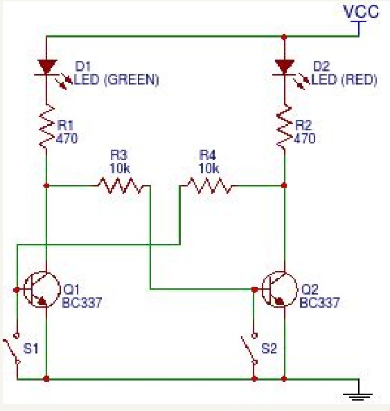
Bloody horrible isn’t it!! This is a simple SR Flip-Flop
This is a code block.
10 for a=1 to 20
20 print a